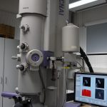
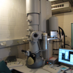
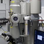
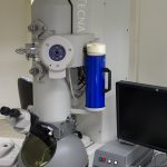
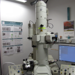
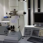
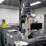
Modern transmission electron microscopes (TEM) are versatile instruments that have been essential for many years in structural and spectroscopic characterization of nanomaterials. TEMs provide analyses of structure and chemical composition over several orders of magnitude, from the millimeter to the atomic scale, under various conditions such as at the boiling point of nitrogen (-195 C), the melting point of gold (~ 1,000 C) or in vitrified water. Likewise, there is a vast range of samples that can be analyzed at EMZ-M using TEM:
- Thin sections of bulk materials such as steel
- Cross-sections of semiconductor components from micro- and nano electronics
- Powder samples e.g. of pharmaceutical compounds
- Nanoparticles and nanostructures such as coatings, needles, or fullerenes
- Native biological macromolecules in aqueous solution
- Sections e.g. of co-polymers
In the TEM labs at EMZ-M, infrastructure is provided for a multitude of analysis techniques aiming at different sample properties, in 2D and 3D:
- Cryo electron microscopy of aqueous samples
- Automated (cryo) electron tomography and 3D reconstruction
- Electron diffraction and automated diffraction tomography (ADT)
- High-resolution scanning TEM (STEM)
- Electron energy loss spectroscopy (EELS)
- Energy-dispersive x-ray spectroscopy
- Spatially resolved spectroscopy by combined STEM + EDX / EELS
For these experimental techniques, we maintain a pool of specialized TEM sample holders:
- Tomography holders with double tilt axes
- Heating and cooling holders ranging from -190 to ~ 1,000 C
- Cryo transfer holders
- Low-background spectroscopy holders
